Wave soldering is a large-scale soldering process by which electronic components are soldered to a printed circuit board (PCB) to form an electronic assembly. The name is derived from the use of waves of molten solder to attach metal components to the PCB. The process uses a tank to hold a quantity of molten solder; the components are inserted into or placed on the PCB and the loaded PCB is passed across a pumped wave or waterfall of solder. The solder wets the exposed metallic areas of the board (those not protected with solder mask, a protective coating that prevents the solder from bridging between connections), creating a reliable mechanical and electrical connection. The process is much faster and can create a higher quality product than manual soldering of components.
Wave soldering is used for both through-hole printed circuit assemblies, and surface mount. In the latter case, the components are glued by the placement equipment onto the printed circuit board surface before being run through the molten solder wave.
Common Types of Soldering Defects
Pin Holes & Blow Holes on a Printed Circuit Board
Pin holes or blow holes are the same thing and caused by the printed board outgassing during soldering. Pin and blow hole formation during wave soldering is normally always associated with thickness of copper plating. Moisture in the board escapes through either thin copper plating or voids in the plating. The plating in the through hole should be a minimum of 25um to stop the moisture in the board turning to water vapor and gassing through the copper wall during wave soldering.
The term pin or blow hole are normally used to indicate the size of the hole, pin being small. The size is solely dependent on the volume of water vapor escaping and the point the solder solidifies.
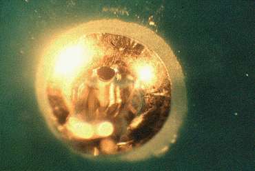
Figure 1: Blow Hole
The only way to eliminate the problem is improve the board quality with a minimum of 25um of copper plating in the through hole. Baking is often used to eliminate the gassing problems by drying out the board. Baking the board takes the water out of the board, but it does not solve the root cause of the problem.
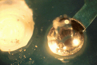
Figure 2: Pin Hole
The test is used to evaluate printed circuit boards with plated through holes for outgassing. It indicates the incidence of thin plating or voids present in through hole connections. It may be used at goods receipt, during production or on final assemblies to determine the cause of voids in solder fillets. Provided that care is taken during testing the boards may be used in production after test without any detriment to the visual appearance or the reliability of the final product.
· Sample printed circuit boards for evaluation
· Canada Bolson oil or a suitable alternative that is optically clear for visual inspection and can be easily removed after test
· Hypodermic syringe for application of oil in each hole
· Blotting paper for removing excess oil
· Microscope with top and underside lighting. Alternatively, a suitable magnification aid of between 5 to 25x magnification and a light box
· Soldering iron with temperature control
1. A sample board or part of a board is selected for examination. Using a hypodermic syringe, fill each of the holes for examination with optically clear oil. For effective examination, it is necessary for the oil to form a concave meniscus on the surface of the hole. The concave form allows an optical view of the complete plated through hole. The easy method of forming a concave meniscus on the surface and removing excess oil is to use blotting paper. In the case of any air entrapment being present in the hole, further oil is applied until a clear view of the complete internal surface is obtained.
2. The sample board is mounted over a light source; this allows illumination of the plating through the hole. A simple light box or illuminated bottom stage on a microscope may provide suitable lighting. A suitable optical viewing aid will be required to examine the hole during test. For general examination, 5X magnification will allow viewing of bubble formation; for a more detailed examination of the through hole, 25X magnification should be used.
3. Next, reflow the solder in the plated through holes. This also locally heats the surrounding board area. The easiest way to do this is to apply a fine-tipped soldering iron to the pad area on the board or to a track connecting to the pad area. The tip temperature can be varied, but 500°F is normally satisfactory. The hole should be examined simultaneously during application of the soldering iron.
4. Seconds after the complete reflow of the tin lead plating in the through hole, bubbles will be seen emanating from any thin or porous area in the through plating. Outgassing is seen as a constant stream of bubbles, which indicates pin holes, cracks, voids or thin plating. Generally if outgassing is seen, it will continue for a considerable time; in most cases it will continue until the heat source is removed. This may continue for 1-2 minutes; in these cases the heat may cause discoloration of the board material. Generally, assessment can be made within 30 seconds of application of heat to the circuit.
5. After testing, the board may be cleaned in a suitable solvent to remove the oil used during the test procedure. The test allows fast and effective examination of the surface of the copper or tin/lead plating. The test may be used on through holes with non tin/lead surfaces; in the cases of other organic coatings, any bubbling due to the coatings will cease within a few seconds. The test also provides the opportunity to record the results both on video or film for future discussion.
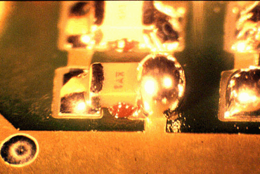
Bulbous Joint / Excess Fillet on a Printed Circuit Board
A solder joint on chip components that is over the height of the part with a convex meniscus is referred to as bulbous or excess fillet. It is caused during separation of the board from the solder wave and is more common in nitrogen soldering.
Cracked Joint on a Printed Circuit Board
Cracking of a solder joint on a plated through joint is uncommon; in Figure 1 the solder joint is on a single-sided board. The joint has failed due to expansion and contraction of the lead in the joint. In this case the fault lies with the initial design as the board is not meeting the requirements of its operating environment. Single-sided joints can fail during assembly due to poor handling but in this case the surface of the joint shows stress lines which have been produced during repeated movement.
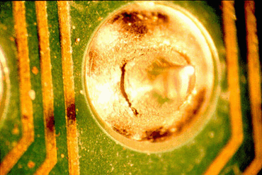
Figure 1: Stress lines here indicate that this crack on a single-sided board was caused by repeated movement during processing.
Figure 2 shows a crack around the base of the fillet and has separated from the copper pad. This is most likely to be related to the basic solderability of the board. Wetting between the solder and the pad surface has not occurred leading to joint failure. Cracking of joints would normally occur due to the thermal expansion of a joint and this would relate to the original design of the product. It is not very common for failures to occur today due to the experience and pre testing conducted by many leading electronics companies.
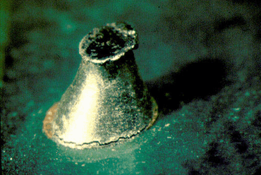
Figure 2: Lack of wetting between the solder and the pad surface caused this crack at the base of a fillet.
Lifted components can occur during wave soldering for a number of reasons. In the case of Figure 1, the part lifted due to the thermal demand on the leads. Simply by increasing the immersion time in the wave eliminated the problem. On lambda style waves it is possible to increase the contact time by adjusting the back wave section which eliminates the need to slow down the conveyor. Slowing down the process does not go down well with production managers. Generally components lift due to: Incorrect lead length causing the leads to hit the solder bath and lift during entry to the wave. Flexure of the board which is commonly seen on large connectors, IC sockets or large IC packages. Basically the board flexes and the component remains still. Light components are lifted by the turbulent wave used for surface mount applications. Components with either different thermal demands or different lead solderability can also cause the lifting seen during wave contact. Although not associated with the wave, vacuum formed shrinkwrap may cause lifting during wave contact. The shrink wrap is some times used to hold components on the surface of the board for lead cutting. It can be pulled under the leads which causes components to lift during wave contact.
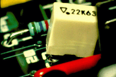
Figure 1: Increasing the immersion time in the wave stopped this problem from occurring.
In the case of Figure 2, the part was not inserted correctly prior to entering the soldering process. It is uncommon for IC packages of this size to lift during wave contact. Generally components lift due to: Incorrect lead length causing the leads to hit the solder bath and lift during entry to the wave. Flexure of the board which is commonly seen on large connectors, IC sockets or large IC packages. Basically the board flexes and the component remains still. Light components are lifted by the turbulent wave used for surface mount applications. Components with either different thermal demands or different lead materials. If a lead is slow to wet due to the thermal demand of the component it can lift in the plated through hole and not sit back on to the surface of the board.

Figure 2: This defect originated in the assembly process, when the part was inserted incorrectly.
Flux Residues on a Printed Circuit Board
Flux residues visible on the board are more common due to the reduction in the use of cleaning in the industry. Over 75% of companies in Europe use no clean low residue materials. With the reliability of no clean being demonstrated in automotive products, the number of cleaning processes will continue to decline.
In Figure 1, the residues are either a result of the formulation of the flux or due to poor process conditions. Many no clean materials rely on the correct pre-heat temperature helping to minimize the residues left on the board. Wave contact time may also affect the residues left on the board. Discussion with the flux supplier should provide the correct process parameters.
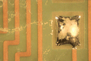
Figure 1: The flux residues here could have been caused by the formulation of the flux or by poor process conditions.
Incomplete Joints on a Printed Circuit Board
The incomplete solder fillet is often seen on single-sided boards after wave soldering.
In Figure 1, the lead-to-hole ratio is excessive, which has made soldering difficult. There is also evidence of resin smear on the edge of the pad. It may be possible, even on this design, to improve the soldering performance by decreasing the conveyor angle from 6 to 4°. This reduces the drainage performance of the wave but can lead to the incidence of shorting. Reducing wave temperature has also been seen to overcome the problem.
As a guide, the hole-to-lead ratio is normally the lead diameter plus 0.010", which is the normal guideline for automatic insertion.
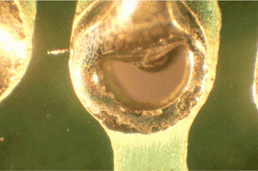
Figure 1: The lead-to-hole ratio here was excessive.
Incomplete solder fillets are caused by poor hole-to-lead ratio, steep conveyor angles, excessive wave temperature and contamination on the edge of the pads.
The example shown in Figure 1 is a result of burring on the copper pads. During either drilling or punching, the copper on the surface of the board was deflected in some areas, making soldering difficult. The same thing can occur if resin is smeared onto the edge of the pads.
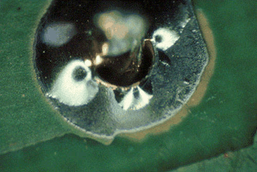
Figure 2: Burring on the copper pads caused this defect.
The solder has not fully filled the plated through hole in Figure 1. This is due either to the pre-heat being set too low or poor flux application. In both cases, a check on the process parameters should eliminate the problem.
This is a common problem seen when a company changes over from a foam fluxer to a spray flux unit; it is due to the poor penetration of flux into the through hole.
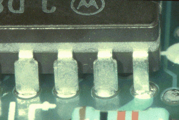
Figure 1: Solder has not fully filled the plated through hole here.
Poor or incomplete hole fill is normally a fluxing or heating issue. It is uncommon for it to be a printed board problem. In Figure 2, the poor hole fill is due to pre heat settings. The solder has wetted the leads of the device but failed to wet the surface of the through hole.
As a guide, the topside temperature of the printed board just before wave contact should be 100-110°C. This is generally true for double sided and multilayer boards. Single-sided boards will be processed at slightly lower temperatures as no solder penetration is needed.
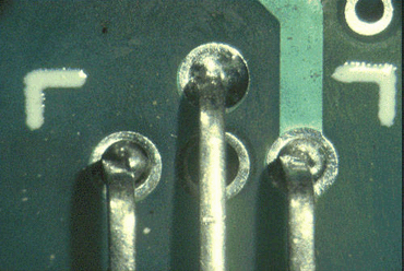
Figure 2: The solder has failed to wet the surface of the through-hole here.
The solder has not fully filled the plated through hole in Figure 3. This is either due to the pre heat operation being set too low or poor flux application. In both cases a check on the process parameters should eliminate the problem.
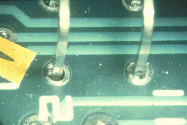
Figure 3: The solder has not fully filled the plated through hole on the left.
In Figure 4, one hole has filled and the second has not, which should indicate the problem is less likely to be a printed board problem. Close examination shows that the solder has solidified on one hole due to the thermal demand of the component. By raising the pre heat or by increasing wave contact time this problem should be simply overcome.
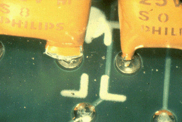
Figure 4: One hole has filled; the other has not.
Poor hole fill can be caused by incorrect pre heat, no flux or a total miss of the solder wave. In Figure 5 there is no evidence of solder in the through hoes or vias. It is more than likely that the board failed to make contact with the wave which could be due to wave height, damaged fingers or pallets not being maintained. Incorrect loading of the board in to the systems may also have caused this fault.
It is possible that the quality of the through hole plating may have been responsible, but this is less likely to be the case as it would be very apparent on other boards in the batch.
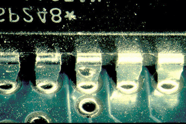
Figure 5: It is likely that this board failed to make contact with the wave.
The example of poor hole fill in Figure 6 is fairly unique as the problem is due to the legend on the printed board. Close examination shows that poor design rules have allowed the legend to contaminate the top of the plated through holes. The solder has failed to rise in the hole or wet across the surface of the pads. In this case there is no benefit from the legend and new design rules need to be applied.
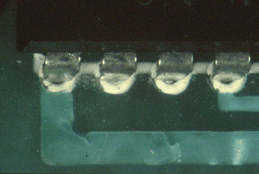
Figure 6: The legend on this PCB has contaminated the top of the plated through holes.
Figure 7 shows poor wetting of the surface of the pads and is likely to be due to the thickness of the tin/lead coating. Solder leveling often leaves a thin deposit on the surface of the pads and on the edge of the hole. This defect is often referred to as the weak knee effect, where the solder fails to wet over the knee of the hole and on to the pads. Poor hole fill can also be due to the pre-heat operation being set too low or poor flux application. In both cases a check on the process parameters should eliminate the problem.
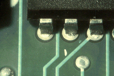
Figure 7: An example of the “weak knee” effect.
Joint Contamination on a Printed Circuit Board
The top of the plated through hole in Figure 1 has been contaminated during the soldering operation. The temperature has caused the coating on the resistor network to soften and has contaminated the board surface. During pre heat the top board temperature would normally be 100-110°C and may well reach over 190°C when contacting the wave. The component should not have caused this problem if normal process conditions are maintained. The component should be reassessed for process compatibility.
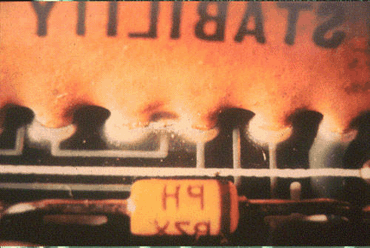
Figure 1: The lead-to-hole ratio here was excessive.
Lifted Pads on a Printed Circuit Board
Lifted pads are rarely seen on plated through hole boards but can occur on single-sided boards during assembly. The example in Figure 1 occurred directly after wave soldering when the assembly was being handled. The adhesion of the copper foil decreases as the surface heats up so directly after soldering the copper adhesion can be low. Any handling or force applied to the components can cause lifting of the pads. Care needs to be taken when lifting boards from the conveyor or out of pallets as often large components are often used by operators as handles.
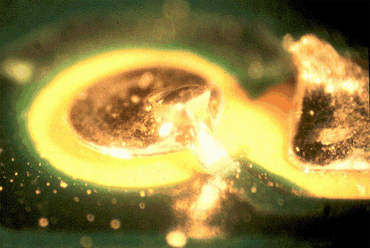
Figure 1: This lifted pad occurred during handling, right after wave soldering.
Lifted Resist on a Printed Circuit Board
Figure 1 shows a very obvious example of resist lifting from the surface of the board after soldering. Quite simply this is due to incorrect specification of the printed board. Tin/lead should not be used under resist on professional circuit boards. As the tin/lead moves into a liquid phase it expands and may cause loss of adhesion between the solder and the resist. If the resist is brittle or thin it will separate as shown in Figure 1. It is possible to use tin/lead if the thickness of the coating is less than 3-5µm as there will be very little movement during wave or reflow soldering.
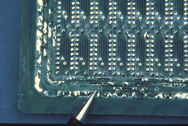
Figure 1: The resist lifting here is due to incorrect specification of the PCB.
Pad Contamination on a Printed Circuit Board
The solder joints shown in Figure 1 are satisfactory, but the solder resist on the pads has resulted in a reduction in the solder volume. The resist on the board is directly related to the poor design rules used on this printed board. The correct design rules for resist apertures are a 0.002-0.003" annulus ring around the pads. This clearance is necessary to allow for misalignment on the board during fabrication.
The example in Figure 1 has been designed with resist apertures smaller than the pad size. It is worth pointing out that during wave soldering the resist on the pad may affect the visual appearance of the joints but it will not cause any problems of reliability. Using a reduced resist aperture has been used in the past by the author to eliminate solder shorting. Sometimes it is not always possible to eliminate problems simply with changes to process parameters. As an alternative, when all else fails and when the design engineer does not want to change the design, use a glue dot. Ask your placement engineers to program in an extra glue dot between the lead which always shorts, this will be a simple fixit.
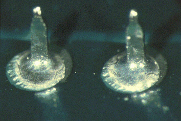
Figure 1: Here, the resist apertures are smaller than the pad size.
Efficient Technology Co., Ltd provide a full SMT assembly line solutions, including SMT Assembly Line, Pick and place machine, Insert Plug-in machine, SMT Reflow oven, Wave Soldering Machine, SMT Stencil Printer, SMT Inspection machine, SMT Peripheral Equipment, SMT Spare Parts etc any kind SMT machines you may need, please Contact us for more information: wechat:+86 13714564591, Skype:sales@effsmt.com, Email: sales@effsmt.com

Contact: Jacky
Phone: +8613714564591
E-mail: sales@effsmt.com
Add: No. 4, Yangyong Industrial Zone, Shapu Community, Songgang Street, Baoan District, Shenzhen